
The Gaps In The New China Lithography Restrictions – ASML, SMEE, Nikon, Canon, EUV, DUV, ArFi, ArF Dry, KrF, and Photoresist
新中国光刻限制的缺口 – ASML、SMEE、尼康、佳能、EUV、DUV、ArFi、ArF 干式、KrF 和光刻胶

The economic cold war rages on. Decades of state-sponsored corporate espionage, hacking, dumping, and draconian restrictions including forced tech transfers for market access from China have led to retaliatory sanctions on China’s access to the 21st century’s most important industry, semiconductors. In October, the US imposed restrictions on AI chips and semiconductor manufacturing equipment, but it did not fully address all concerns.
经济冷战持续加剧。数十年来,国家支持的企业间谍活动、黑客攻击、倾销以及包括强制技术转让以获得市场准入的严厉限制,导致了对中国进入 21 世纪最重要行业——半导体的报复性制裁。10 月份,美国对人工智能芯片和半导体制造设备实施了限制,但并未完全解决所有问题。
Over the last few months, a few of these were partially addressed, but they haven’t closed the biggest gaps. The US is the leader in wafer fabrication equipment with a majority share in deposition, etch, process control, CMP, and ion implantation, but many US equipment makers, such as Applied Materials, Lam Research, and KLA, have complained that US restrictions would allow overseas competitors such as the Dutch ASM International and Japanese Tokyo Electron to gain market share and blunt the impact of the technology restrictions.
在过去几个月中,这些问题中的一些得到了部分解决,但并没有填补最大的空白。美国在晶圆制造设备方面处于领先地位,在沉积、刻蚀、工艺控制、化学机械抛光(CMP)和离子注入等领域占据了大部分市场份额,但许多美国设备制造商,如应用材料公司、拉姆研究公司和 KLA,抱怨美国的限制将使海外竞争对手,如荷兰的 ASM 国际和日本的东京电子,获得市场份额,并削弱技术限制的影响。
Furthermore, the world’s largest equipment maker, ASML, has been dogmatic about not following US technology restrictions.
此外,全球最大的设备制造商 ASML 对不遵循美国技术限制持坚定态度。
As a European-based company with limited US technology in our systems, ASML can continue to ship all non-EUV lithography systems to China out of the Netherlands.
作为一家总部位于欧洲的公司,ASML 在我们的系统中拥有有限的美国技术,可以继续从荷兰向中国发运所有非极紫外光(EUV)光刻系统。
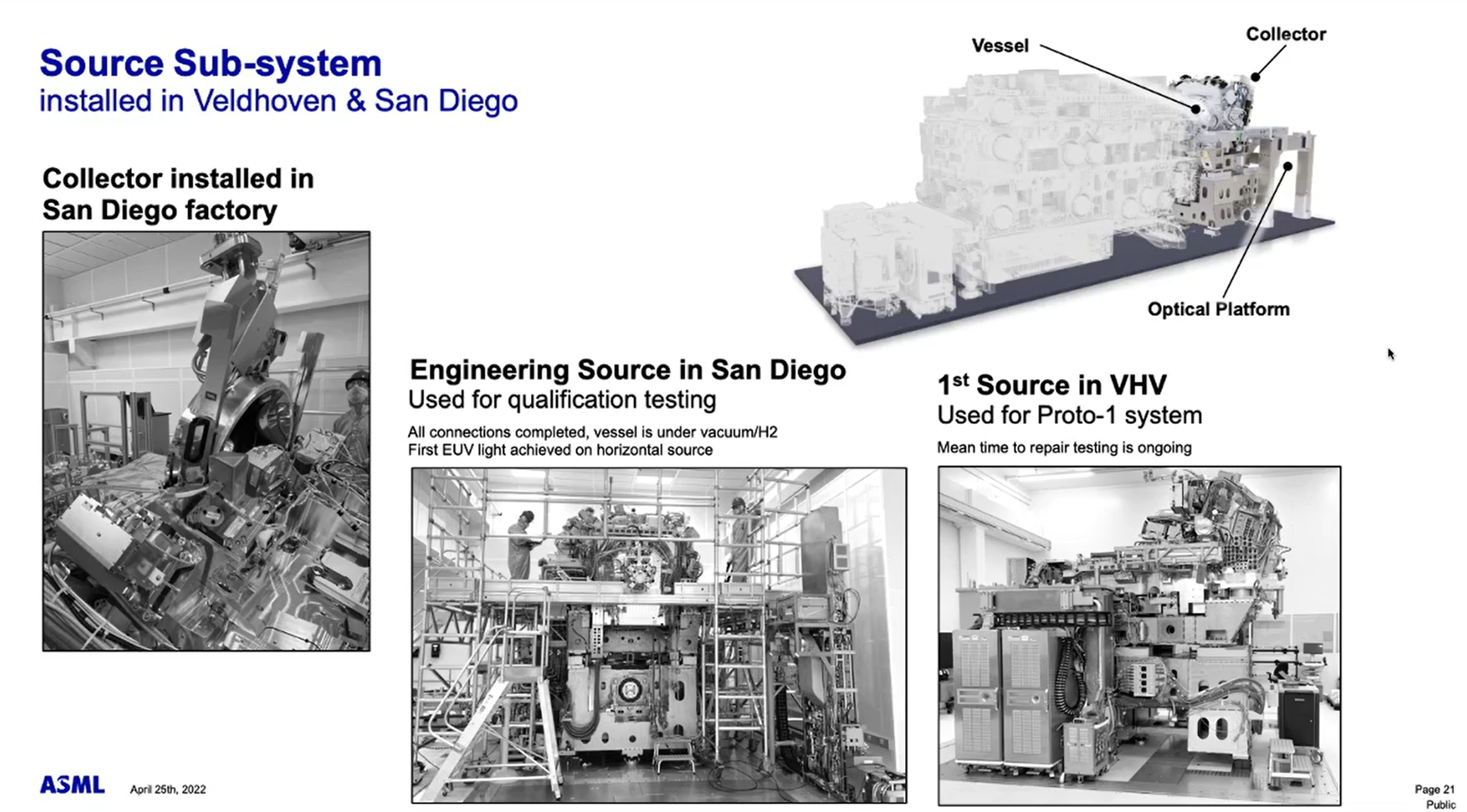
This is despite ASML’s source engineering being done in San Diego by a US company they acquired, Cymer.
尽管 ASML 的源工程是在他们收购的美国公司 Cymer 位于圣地亚哥进行的。
Furthermore, mask-related and OPC software required to operate lithography tools is also engineered in the US. While the US certainly has options to make ASML comply with technology restrictions due to its high US-based technology content, the US has chosen the diplomatic route.
此外,操作光刻工具所需的掩模相关和 OPC 软件也在美国研发。虽然美国确实有选择使 ASML 遵守技术限制的选项,因为其高美国技术含量,但美国选择了外交途径。
The US, Japan, and the Netherlands have been hosting discussions to restrict China’s access to lithography equipment over the last few months. On Friday, news broke that the three countries agreed to certain restrictions on lithography equipment. The question remains, how far do these restrictions go, and what do they contain? Our understanding is that these restrictions are extremely limited and only regard ArFi tools. This agreement is still verbal in nature, but we believe the 3 countries have agree to move forward on this basis. Some other non-lithography tools are also supposedly included. Today we are going to discuss the many gaping holes in the newly agreed lithography restrictions regarding equipment, chemicals, and component supply chains.
美国、日本和荷兰在过去几个月中一直在举行讨论,以限制中国获取光刻设备。周五,消息传出这三个国家达成了对光刻设备的某些限制。问题是,这些限制的范围有多大,内容是什么?我们了解到,这些限制非常有限,仅涉及 ArFi 工具。该协议仍然是口头性质,但我们相信这三个国家已同意在此基础上继续推进。还有一些其他非光刻工具也 supposedly 包括在内。今天我们将讨论新达成的光刻限制在设备、化学品和组件供应链方面的许多漏洞。
Equipment Supply Chain 设备供应链
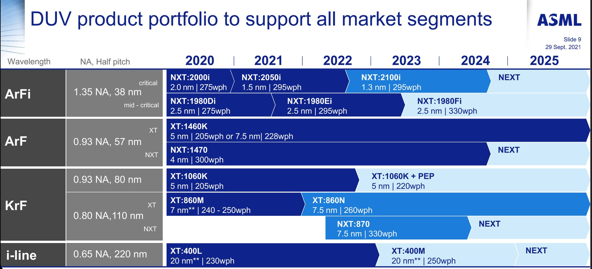
The primary avenue to restrict China’s access to semiconductors is with equipment. While there is a tri-lateral agreement for blocking access to DUV lithography, there is no mention of how far back this goes. DUV is a very broad technology that includes Krypton fluoride (KrF), Argon Fluoride (ArF), and Argon Fluoride Immersion (ArFi) lithography.
限制中国获取半导体的主要途径是通过设备。虽然有三方协议阻止对 DUV 光刻的访问,但没有提到这项限制的追溯时间。DUV 是一种非常广泛的技术,包括氟化氪(KrF)、氟化氩(ArF)和氟化氩浸没(ArFi)光刻。
Nikon released the first DUV tool called NSR-1505EX in 1988 using KrF lithography. It initially had a resolution of 500nm, but over time it was upgraded to be capable of 250nm with an overlay of 100nm. The newly agreed restrictions by the US, Netherlands, and Japan does not cover technology this old. On the other hand, ASML’s NXT 2100i, released in 2022, has an overlay of 1.5nm and can pattern the minimum features required for advanced nodes.
尼康于 1988 年发布了第一款 DUV 工具 NSR-1505EX,采用 KrF 光刻技术。最初的分辨率为 500nm,但随着时间的推移,它被升级为能够实现 250nm 的分辨率,叠加误差为 100nm。美国、荷兰和日本新达成的限制不涵盖如此老旧的技术。另一方面,ASML 于 2022 年发布的 NXT 2100i,叠加误差为 1.5nm,能够为先进节点绘制所需的最小特征。
If the goal is to prevent China from acquiring 14nm, 7nm, or 5nm process technologies, then the ban must reach a differing level of tooling capable of processing the features for these nodes. For example, TSMC’s 16nm and 12nm process technologies have a minimum metal pitch of 64nm. TSMC’s 7nm process technology has a minimum metal pitch of 40nm. TSMC’s 5nm process technology has a minimum metal pitch of 28nm.
如果目标是防止中国获得 14nm、7nm 或 5nm 工艺技术,那么禁令必须达到能够处理这些节点特征的不同级别的工具。例如,台积电的 16nm 和 12nm 工艺技术的最小金属间距为 64nm。台积电的 7nm 工艺技术的最小金属间距为 40nm。台积电的 5nm 工艺技术的最小金属间距为 28nm。
Any ban on lithography equipment must consider these minimum metal pitches as the specifications for banning equipment.
任何对光刻设备的禁令必须考虑这些最小金属间距作为禁令设备的规格。
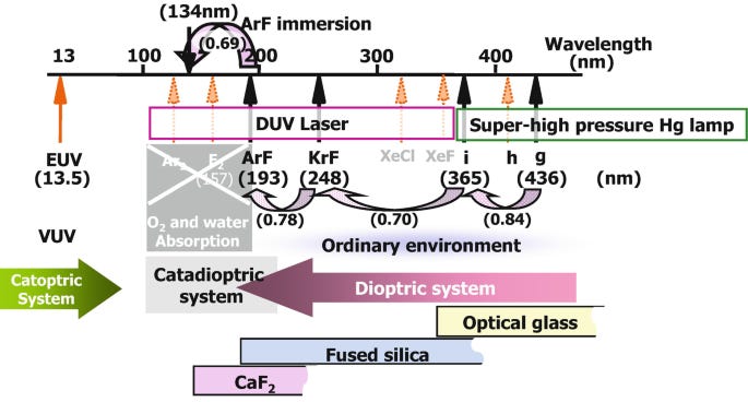
In the Rayleigh criterion equation (CD = k1 • λ / NA), the CD is the critical dimension, the smallest possible feature size. λ is the wavelength of light used. NA is the numerical aperture of the optics, defining how much light they can collect. Finally, k1 (or the k1 factor) is a coefficient that depends on many factors related to the chip manufacturing process. The physical limit lithography is k1 = 0.25.
在瑞利准则方程(CD = k1 • λ / NA)中,CD 是临界尺寸,最小可能的特征尺寸。λ 是使用的光的波长。NA 是光学的数值孔径,定义了它们可以收集多少光。最后,k1(或 k1 因子)是一个系数,取决于与芯片制造过程相关的许多因素。物理极限光刻为 k1 = 0.25。
Self-aligned quad patterning (SAQP) is generally considered the furthest economic way to stretch a DUV lithography generation. While there are more complex schemes for lithography, we will stick to what is economically feasible today. TSMC and China’s SMIC have achieved 7nm process technology, without EUV, using SAQP with argon fluoride immersion (ArFi) lithography, but that isn’t the limit of what’s economically achievable.
自对准四重图案化(SAQP)通常被认为是延伸深紫外(DUV)光刻技术的最经济方式。虽然光刻有更复杂的方案,但我们将坚持今天经济上可行的方案。台积电和中国的中芯国际已经实现了 7nm 工艺技术,未使用极紫外(EUV),而是采用了氟化氩浸没(ArFi)光刻,但这并不是经济上可实现的极限。
The 28nm minimum metal pitch used on TSMC’s N5 could be manufactured without EUV. SAQP using ArFi lithography (NA=1.35, λ=193nm) can produce this feature size at a k1 of 0.391. If the goal is to stop China from achieving 5nm process technology, then ArFi shipments must be blocked. ASML and Nikon can manufacture ArFi lithography tools capable of 28nm minimum metal pitch. While this wouldn’t be as cost-effective as EUV, the delta would not be unachievable for a nation-state like China.
台积电的 N5 所使用的 28nm 最小金属间距可以在没有 EUV 的情况下制造。使用 ArFi 光刻(NA=1.35,λ=193nm)的 SAQP 可以在 k1 为 0.391 的情况下生产此特征尺寸。如果目标是阻止中国实现 5nm 工艺技术,那么必须阻止 ArFi 的出货。ASML 和尼康可以制造能够实现 28nm 最小金属间距的 ArFi 光刻工具。虽然这不会像 EUV 那样具有成本效益,但对于像中国这样的国家来说,这一差距并不是不可实现的。
If the goal is to prevent China from achieving high volume 7nm process technology, then all tools that can achieve a 40nm minimum metal pitch used on TSMC 7nm class process technologies must be blocked. The new restrictions would include ArFi lithography, but they would also need to extend further. SAQP using dry argon fluoride ArF lithography (NA=0.93, λ=193nm) can produce this feature size with a k1 of 0.385. Again, this isn’t going to be as economical as Intel, TSMC, and SMIC’s ArFi DUV “7nm,” but it is achievable, especially given the importance of national security. The cost delta would be significantly less than that of the subsidies for a nuclear power plant in the US.
如果目标是防止中国实现高容量的 7nm 工艺技术,那么必须阻止所有能够在台积电 7nm 级工艺技术上实现 40nm 最小金属间距的工具。新的限制将包括 ArFi 光刻,但还需要进一步扩展。使用干氩氟 ArF 光刻(NA=0.93,λ=193nm)的 SAQP 可以以 0.385 的 k1 生产此特征尺寸。再说一次,这不会像英特尔、台积电和中芯国际的 ArFi DUV“7nm”那样经济,但这是可实现的,特别是考虑到国家安全的重要性。成本差异将显著低于美国核电站的补贴。
If the goal is to prevent China from expanding their high volume 14nm process technology, then all tools that can achieve a minimum metal pitch of 64nm used on nodes, such as TSMC’s 16nm and 12nm and Samsung’s 14nm, must be blocked. Not only should these restrictions, if adequately enforced, include ArF lithography tools, but they would also need to extend further to some types of Krypton fluoride (KrF) tools. Krypton fluoride has a λ=248nm, but there were multiple generations of the lens stack. In each generation, NA improved from 0.6 to 0.8 to 0.93.
如果目标是防止中国扩展其高容量的 14nm 工艺技术,那么所有能够在节点上实现最小金属间距为 64nm 的工具,例如台积电的 16nm 和 12nm 以及三星的 14nm,必须被阻止。这些限制如果得到充分执行,不仅应包括 ArF 光刻工具,还需要进一步扩展到某些类型的氟化氪(KrF)工具。氟化氪的波长为λ=248nm,但镜头堆叠有多个世代。在每一代中,数值孔径(NA)从 0.6 提高到 0.8,再到 0.93。
SAQP using the most advanced KrF lithography (NA=0.93, λ=248nm), can produce this feature size with a k1 of 0.48. SAQP using the mid-range KrF lithography (NA=0.8, λ=248nm), can create this feature size with a k1 of 0.413. These are very achievable with tools from ASML, Nikon, or Canon. Again, the economics here would not be optimal, but even doubling lithography costs on a 14nm class node would only lead to a ~19% increase in cost for each wafer. This is already economically viable with the level of state subsidies China gives their domestic firms.
SAQP 使用最先进的 KrF 光刻技术(NA=0.93,λ=248nm),可以以 k1 为 0.48 的参数生产此特征尺寸。SAQP 使用中档 KrF 光刻技术(NA=0.8,λ=248nm),可以以 k1 为 0.413 的参数创建此特征尺寸。这些在 ASML、尼康或佳能的设备上都是非常可行的。再次强调,这里的经济性并不是最优的,但即使在 14nm 级节点上将光刻成本翻倍,每片晶圆的成本也只会增加约 19%。这在中国对其国内企业提供的国家补贴水平下,已经是经济上可行的。
We should note that regulators should also look to the overlay specification when determining which tools to restrict. In lithography, overlay refers to the alignment accuracy between different layers during manufacturing. It is the positional accuracy with which one layer is aligned to another layer. Each of our examples utilized self-aligned quad patterning (SAQP), meaning 4-layers of lithography need to be aligned. As such, overlay control is critical.
我们应该注意,监管机构在确定限制哪些工具时,也应考虑叠加规范。在光刻中,叠加是指在制造过程中不同层之间的对齐精度。它是一个层与另一个层之间的定位精度。我们每个例子都采用了自对准四重图案化(SAQP),这意味着需要对齐 4 层光刻。因此,叠加控制至关重要。
ASML’s most advanced EUV steppers have an overlay accuracy of 1.1nm. The prior version, 3400C, which was the primary EUV tool they shipped in 2021, has an overlay accuracy of 1.5nm. This is worse than ASML’s most advanced DUV tool, 2100i. For today, we won’t dive too much into where we believe the line for overlay accuracy on 14nm, 7nm, and 5nm sits for export controls, as that would be far too much into the weeds for most readers.
ASML 最先进的 EUV 步进机的叠加精度为 1.1nm。之前的版本 3400C 是他们在 2021 年出货的主要 EUV 工具,叠加精度为 1.5nm。这比 ASML 最先进的 DUV 工具 2100i 要差。今天,我们不会深入探讨我们认为 14nm、7nm 和 5nm 的叠加精度在出口管制中的界限,因为这对大多数读者来说过于复杂。
Chemical Supply Chain 化学供应链
The next gap in the new export controls is the chemical supply chain, namely photoresist. We did a deep dive into photoresist here, but the summary is that lithography tools require photoresists to pattern features on a wafer. The vast majority of the world’s photoresist is manufactured by a handful of Japanese companies, with the US-based Dupont as the distant 4th place competitor. Photoresist chemical compositions involved a lot of fine-tuning with end customers for the type of lithography, process nodes, types of features, and feature sizes in many cases. Furthermore, the equipment used to deposit, develop, and bake photoresist is also entirely Japanese.
新出口管制的下一个空白是化学供应链,即光刻胶。我们对此进行了深入研究,但总结是光刻工具需要光刻胶在晶圆上形成图案。全球绝大多数光刻胶由少数日本公司生产,而美国的杜邦公司则是远远落后的第四名竞争者。光刻胶的化学成分在许多情况下需要与最终客户进行大量微调,以适应光刻类型、工艺节点、特征类型和特征尺寸。此外,用于沉积、显影和烘烤光刻胶的设备也完全是日本制造。
Any country in the world could be blocked from all lithography and, therefore, semiconductor manufacturing if Japan restricted photoresist shipments. The complete lack of restrictions around photoresists represents a significant hole that governmental regulations have not contemplated.
任何国家都可能因日本限制光刻胶的运输而被阻止进行所有光刻和半导体制造。光刻胶完全没有限制的情况代表了一个政府法规未曾考虑的重要漏洞。
There are over a hundred DUV tools already at SMIC alone. These could be reorganized and shifted to fabricate for different process nodes. SMIC could achieve a capacity of well over 100,000 wafers a month of 7nm foundry capacity with their existing DUV tools alone. This is higher than Samsung and Intel’s advanced node (<=7nm) foundry capacity, combined. If all DUV tools at various Chinese nationals such as HuaHong, Shanghai Huali, YMTC, CXMT, GTA Semi, Nexchip, Yandong, Nexperia, CR Micro, Sien, Fulsemi, SEMC, NSEMI were reappropriated by SMIC, the 7nm capacity they could build would far exceed that of even TSMC’s 7nm.
在中芯国际(SMIC) alone 已经有超过一百台 DUV 工具。这些工具可以重新组织并转移以制造不同工艺节点。中芯国际仅凭现有的 DUV 工具就能实现每月超过 100,000 片 7nm 代工能力。这一数字高于三星和英特尔的先进节点(<=7nm)代工能力的总和。如果中芯国际重新利用华虹、上海华力、长江存储、华虹半导体、GTA 半导体、Nexchip、燕东、Nexperia、CR 微电子、Sien、Fulsemi、SEMC、NSEMI 等各家中国企业的所有 DUV 工具,他们能够建立的 7nm 产能将远远超过台积电的 7nm 产能。
It is not enough to only block the shipment of new tools to China if the goal is to limit their manufacture of advanced semiconductors. Shipment of photoresists must also be stopped as Western governments do not know what process node existing DUV tools are being used.
仅仅阻止向中国运输新工具并不足以限制其制造先进半导体。如果目标是限制其制造先进半导体,还必须停止光刻胶的运输,因为西方政府不知道现有的 DUV 工具正在使用哪个工艺节点。
Component Supply Chain 组件供应链
This leads to the final gap, the component supply chain. DUV tools must be regularly serviced with replacement parts by ASML, Nikon, and Canon. The service of these tools must also be blocked if the goal is to contain China’s capacity on leading-edge nodes.
这导致了最后一个差距,即组件供应链。DUV 工具必须定期由 ASML、尼康和佳能进行更换零件的维护。如果目标是限制中国在先进节点的产能,这些工具的服务也必须被阻止。
While China’s lithography champion, SMEE, is on the sanctions list, SMEE has already shipped working I-Line lithography tools. Their argon fluoride DUV lithography is still not production ready for front-end wafer fabrication. This doesn’t mean they cannot catch up. Many firms in ASML’s lithography supply chain, such as Zeiss, continue to expand in China with joint ventures and technology transfers. Given the civil-military fusion of China, it would be straightforward for these technologies to slip through the cracks into SMEE’s control.
尽管中国的光刻机冠军 SMEE 在制裁名单上,SMEE 已经发运了可工作的 I 线光刻工具。他们的氩氟 DUV 光刻仍未准备好用于前端晶圆制造。这并不意味着他们无法赶上。ASML 光刻供应链中的许多公司,如蔡司,继续通过合资企业和技术转让在中国扩展。考虑到中国的军民融合,这些技术很容易在 SMEE 的控制下悄然流出。
Lastly, mask related tools also have zero restrictions, which is also a hole.
最后,与口罩相关的工具也没有任何限制,这也是一个漏洞。
The lack of upstream component supply chain restrictions is a significant hole in the trilateral agreement between the US, Japan, and Netherlands. If the goal is to restrict 5nm, 7nm, and 14nm process technologies, KrF and ArF lithograph equipment, photoresist, and subcomponents must all be limited, or else China will be able to reconfigure existing equipment and accelerate domestic development of lithography tools.
上游组件供应链限制的缺失是美国、日本和荷兰三方协议中的一个重大漏洞。如果目标是限制 5nm、7nm 和 14nm 工艺技术,那么 KrF 和 ArF 光刻设备、光刻胶及其子组件都必须受到限制,否则中国将能够重新配置现有设备,加速国内光刻工具的发展。


Good note. Thank you. 好的记录。谢谢。
There is no long term vision for the sanctions. Do we really think with all the scientists and engineers that China has and will have, they won't be producing all these tools? 2 years ago we didn't imagine they would be producing chips at 7nm. I suspect they've been working on them for several years already.
制裁没有长期愿景。我们真的认为,考虑到中国拥有并将拥有的所有科学家和工程师,他们不会生产这些工具吗?两年前我们无法想象他们会生产 7nm 的芯片。我怀疑他们已经在这方面工作了好几年。
If they start building these tools, western supply chain will be devastated.
如果他们开始构建这些工具,西方供应链将会受到严重打击。
10 条由迪伦·帕特尔及其他人回复的内容